Supplement 1.13: Semiconductor photodiodes (2/4)
Structure and Function of a Semiconductor Photodiode
In addition to the currents in a semiconductor diode mentioned on the previous page, photodiodes have a further current that depends on the illumination: the photocurrent . It is proportional to the brightness, which is why photodiodes are very well suited to quantitative light measurements. The following extended Shockley equation applies to the characteristic curve of a photodiode:
The following graph shows how it varies for uniformly increasing illuminance levels.
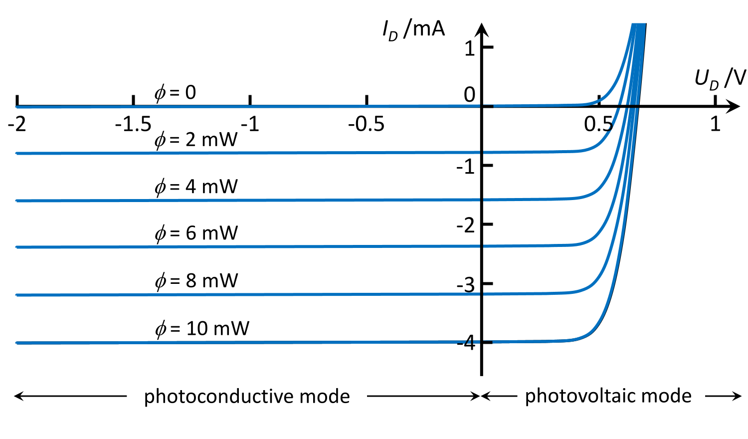
A comparison with the diode characteristic curve on the previous page shows that the forward current in the photodiode graph remains limited to small values. It actually plays a minor role in photodiodes. Due to the difference in polarity, the photocurrent is in the opposite direction to the forward current. Photodiodes are therefore used exclusively in regions of the characteristic curve where the forward current is very small or where the photocurrent dominates.
From the data in the graph, it is possible to estimate the sensitivity S in comparison with vacuum photodiodes and photomultipliers. 10 mW of radiant power yields a photocurrent of approximately 4 mA. Therefore:
This value is about 10 times higher than that of vacuum detectors. This is because a photon absorbed by a vacuum photocathode does not always result in a free electron. In semiconductors, the photoelectrons do not have to escape into the vacuum; they remain within the semiconductor, which significantly improves the efficiency. Thus, the internal photoelectric effect in semiconductors proves to be very advantageous compared with the external photoelectric effect of vacuum photocathodes.
These detectors can be divided into two groups according to their application:
- Solar cells (or: photovoltaic cells) designed to maximise electrical output or efficiency. They operate in photovoltaic mode. Changes in signal over time, such as those caused by changing cloud cover, occur slowly; the cells therefore do not need to be fast. They consist mainly of silicon, but may also be made from other semiconductors or even organic materials, with either a crystalline or amorphous structure. Factors such as efficiency, service life, availability of raw materials and manufacturing costs are the main considerations. These topics will not be explored in further detail here.
- Photodiodes in the strict sense, with the highest possible sensitivity and fast response times, so that even low light levels, high signal frequencies or short laser pulses can be measured. This is achieved using PIN diodes. In PIN diodes, there is an undoped or neutral-doped layer between the p- and n-doped layers: the i-layer. i stands for intrinsic, i.e. intrinsically conductive. The following figure shows the structure of these diodes. However, pn photodiodes are also commonly used, as they produce less noise than PIN diodes when operated without bias (i.e. in short-circuit mode).
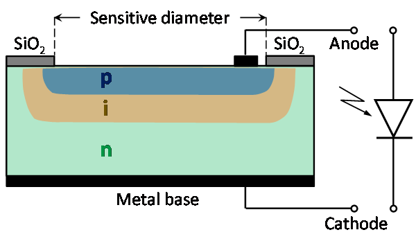
An external voltage applied in the reverse direction (photoconductive mode) draws the mobile charge carriers out of the i-layer, which consequently behaves like an insulator. The electric field created by the external voltage is therefore confined to the i-layer. When light is applied, the internal photoelectric effect generates electrons and hole carriers in the i-layer. The electric field accelerates the electrons very rapidly towards the p-layer and the hole carriers towards the n-layer; they pass through these layers, reach the electrical terminals of the diode and are available as photocurrent. Without an electric field in the i-layer, the charge carriers would reach the terminals via slow diffusion. This increases the rate of undesirable recombination of electrons and hole carriers, thereby reducing the diode’s sensitivity.
From an electrical point of view, the photodiode is similar to a plate capacitor, with the two plates consisting of the p- and n-layers of the semiconductor. The creation of a region depleted of charge carriers in the i-layer by the external voltage behaves in a similar way to the separation of the capacitor plates, which leads to a reduction in capacitance. This enables higher cut-off frequencies for the measurement of high-frequency light signals.