Supplement 1.13: Semiconductor photodiodes (1/4)
Semiconductor diodes
Semiconductor diodes, which include photodiodes, are usually made of tetravalent silicon. The addition of impurity atoms allows the current flow to be specifically controlled. With pentavalent elements, an excess of freely moving electrons is obtained in the semiconductor. With trivalent elements, there is a deficit of electrons; the missing electron sites can be filled by neighbouring electrons; the sites thus vacated move through the semiconductor like electrons with a positive charge; they are called hole carriers. The addition of such elements is referred to as doping: pentavalent elements result in n-type doping, where n denotes the free electrons with a negative charge. Trivalent elements result in p-type doping due to the freely mobile electron holes with a positive charge.

If both doped regions are created in different areas of the same crystal and both areas are connected to wires, the result is a semiconductor diode with the circuit symbol shown on the right. The p-doped side forms the anode, and the n-doped side forms the cathode. If the positive terminal of a voltage source is connected to the anode and the negative terminal to the cathode, the diode conducts current (forward direction); with reverse polarity, it blocks the current (reverse direction). For a detailed explanation of the underlying physics, please refer to the literature on semiconductor physics.
An idealised model of the semiconductor diode yields a current-voltage characteristic (voltage-current curve) with an exponential curve. This is the Shockley equation
which describes the relationship between the diode current and the voltage across the diode. The graph in the right-hand column illustrates this curve.
For sufficiently negative reverse voltages, the exponential function approaches zero and . The quantity is a reverse current, which for silicon diodes is approximately 10 pA and results in a negative diode current of the same magnitude. It is temperature-dependent and increases exponentially as the temperature rises. For photodiodes, it may therefore be useful to cool them in order to keep the dark current low when measuring low light levels.
The quantity is referred to as the temperature voltage, as the following applies: , where is the absolute temperature, is the Boltzmann constant, and is the elementary charge. At room temperature , .
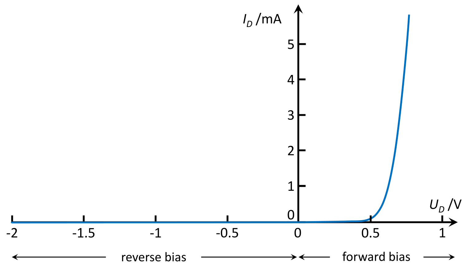
For current to flow in the forward direction, a minimum voltage (the forward voltage) is required, which depends on the type of semiconductor; for silicon, this is approximately 0.7 V. The characteristic curve also depends on temperature in the forward direction: it shifts to the left by approximately 2 mV for every degree increase in temperature. Diodes should therefore not be operated at constant forward voltages: as the temperature rises, the diode current would increase, which in turn would lead to higher temperatures and, consequently, a further increase in current, resulting in the diode destroying itself due to overheating.
The characteristic curves of real diodes may deviate significantly from this idealised curve:
- The ohmic resistance of the semiconductor is not taken into account in the Shockley equation. In power diodes and for high currents, a higher forward voltage is required due to this resistance.
- The reverse current in real diodes is actually around 10 nA at room temperature, around 10 μA at 100°C,and also increases as the reverse voltage rises. Both phenomena are caused by surface defects in the semiconductor: the edge of the crystal always represents a disruption in the crystal lattice.
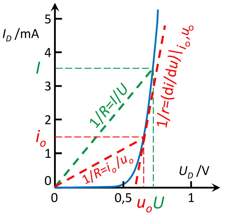
The properties described also apply equally to photodiodes. Photodiodes are likewise operated in both the reverse and forward directions. Silicon is particularly suitable for measurements in the visible spectrum. Silicon carbide (SiC) is suitable for the ultraviolet range from 200 to 400 nm. In the near-infrared, germanium (Ge) and the ternary semiconductor indium gallium arsenide (InGaAs) are used, whilst in the mid-infrared, lead sulphide (PbS) is used. The electrical properties of diodes made from these materials differ from those of silicon, but they also exhibit diode behaviour.